-
+ 86-156 60188203
[email protected] - ต้าไจ เมืองหนานหยาง มณฑลเหอหนาน ประเทศจีน
- จันทร์ - เสาร์ 8.00 - 18.00 วันอาทิตย์ปิด
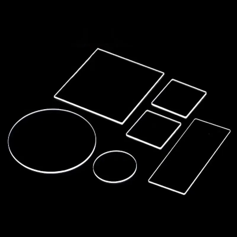
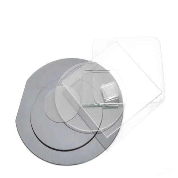
Fused quartz wafers are complex materials that are used in countless modern technology applications. Their uniqueness, however, is their ability to endure very high temperatures. They are also resistant to chemicals, so do not get damaged such easily. Due to these key characteristics, หน้าต่างซิลิกาหลอมรวม find wide applications in many different industries.
Many fields of science and technology use fused quartz wafers. These wafers are primarily used to manufacture semiconductor devices. Semiconductor devices are essential components of computers and many other electronics we use every day. You need materials that are extremely clean and pure for these devices to work effectively. Fused quartz wafers are highly suitable for this task since they are produced from high purity with no dust or any other impurities.
The exception provides great thermal stability. Which means they can then be made into the microchips that run computers and other electronics. They are tiny circuits that can store and process information. They are important components in many electronics we use today including televisions, smart phones and tablets. The manufacturers use หน้าต่างซิลิก้าฟิวส์ยูวี to ensure that these microchips function efficiently and reliably.
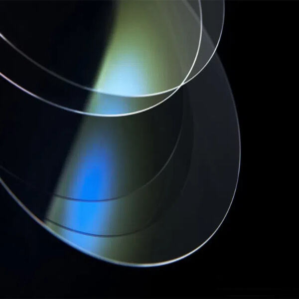
Fused quartz wafers has also some great properties which are really helpful in optics and photonics field. Photonics is the science of using light to carry information or data. These wafers can be clear, allowing light to pass through them. This quality makes them ideal for use in light-dependent devices like lenses and lasers. Their relatively high refractive index enables them to bend light in a highly controlled fashion, allowing for the propagation of clear images and signals.
Fused quartz wafers can withstand very high temperatures this is another key quality. They are also able to withstand temperatures of 1,000 degrees Celsius without breaking or being damaged. This renders them ideal for industrial operations such as furnace tubes, that are used to contain material that is heated to high degrees. They’re also key in laboratory equipment used at high temperatures, such as the analytical and spectroscopic tools that scientists use to study materials.
Fused quartz wafers have several environmental benefits as well as their many industrial applications. They are made from natural materials, meaning they don't carry harmful chemicals that could damage our health or the environment. They can also be recycled, so rather than being discarded after using them, they can be processed and remade into new products! This ability to be recycled helps minimize waste, and it expands greener technologies.
With ISO9001 well as China's New Technology Enterprise High fused quartz wafers Certificate, CE, SGS, our company more than 300 sets equipment and over 10 research scientists. We assure quality.
Nanyang Jingliang is optical component fused quartz wafers area of 10,000 square meters. The company specializes the processing of optical prism lenses, optical system production, sales. We can satisfy all requirements of optical components
We have a sales after-sales team, which is more 60 employees. Our company has a wealth experience in exports and imports and co-operation, our clients from optical firms as well as universities, research centers, research institutions, etc. From more 30000 across more than 80 countries fused quartz wafers the world.
Our company has the fused quartz wafers creating optical prisms that custom-designed to customer drawings, from small size large size. The number of models that be produced online reached over 400. We have lots of experience processing different items are customized.
ลิขสิทธิ์ © บริษัท Nanyang City Jingliang Optical Technology Co., Ltd. สงวนลิขสิทธิ์ — นโยบายความเป็นส่วนตัว